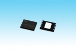
Toshiba Memory Corporation Announces 96-Layer 3D Flash Memory
Fourth Generation Toshiba Memory Corporation BiCS FLASH™ adds layers, boosts capacity
Going forward, Toshiba Memory Corporation will apply its new 96-layer process technology to larger capacity products, such as 512 gigabit (64 gigabytes) and 4-bit-per-cell (quadruple-level cell, QLC) technology, in the near future.
The innovative 96-layer stacking process combines with advanced circuit and manufacturing process technology to achieve a capacity increase of approximately 40% per unit chip size over the 64-layer stacking process. It reduces the cost per bit, and increases the manufacturability of memory capacity per silicon wafer.
Since announcing the world’s first[2] prototype 3D flash memory technology in 2007, Toshiba Memory Corporation has continued to advance development of 3D flash memory and is actively promoting BiCS FLASH™ to meet demand for larger capacities with smaller die sizes.
This 96-layer BiCS FLASH™ will be manufactured at Yokkaichi Operations in Fab 5, the new Fab 2, and Fab 6, which will open in summer 2018.
Note:
[1] A structure stacking flash memory cells vertically on a silicon substrate to realize significant density improvements over planar NAND flash memory, where cells are formed on the silicon substrate.
[2] Source: Toshiba Memory Corporation, as of June 12, 2007.
* Company names, product names, and service names mentioned herein may be trademarks of their respective companies.
View source version on businesswire.com: http://www.businesswire.com/news/home/20170627006606/en/
Website: http://toshiba.semicon-storage.com/ap-en...
Contact
Toshiba Memory Corporation
Business Planning Division
Kota Yamaji
+81-3-3457-3473
semicon-NR-mailbox@ml.toshiba.co.jp
This news is a press release provided by Toshiba Memory Corporation.


