Samsung Readies Green Memory with Advanced Chip Stacking Technology after Extensive System-level Testing
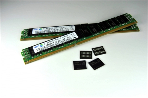
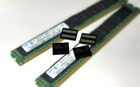
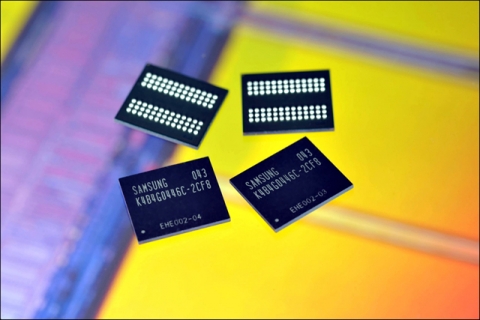
An 8GB RDIMM utilizing Samsung’s 3D TSV technology saves up to 40 percent of the power consumed by a conventional RDIMM. Also, the TSV technology allows for a dramatic improvement in memory chip density that is expected to offset the decrease of memory sockets in next generation server systems. In the face of a 30 percent decrease in memory slots in next-generation servers, the TSV technology will be able to raise the DRAM density by more than 50 percent, making it highly attractive for high-density, high-performance server systems.
Samsung’s TSV technology is a key to solving the paradox of driving lower power consumption in servers, while increasing memory capacity and improving performance.
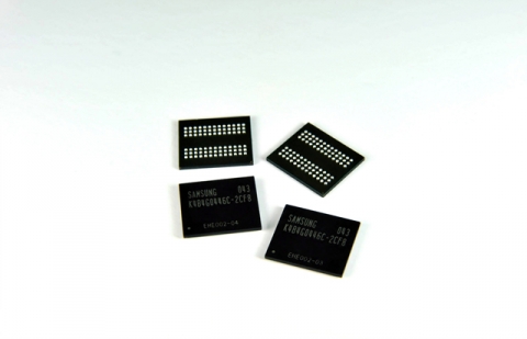
The TSV technology fabricates micron-sized holes through the silicon vertically, with a copper filling. By using the ‘through silicon via’ bonding process instead of conventional wire bonding, signal lines are shortened significantly, enabling the multi-stacked chip to function at levels comparable to a single silicon chip.
Already passing customer performance tests, Samsung is readying its TSV technology for a variety of server applications having stringent performance and power demands.
Increasingly widespread adoption of the 3D TSV technology is expected to take place from 2012. Samsung plans to apply the higher performance and lower power features of its TSV technology to 30nm-class* and finer process nodes.
For more information about Samsung Green DDR3, visit www.samsung.com/GreenMemory
삼성전자 개요
삼성전자는 반도체, 통신, 디지털 미디어와 디지털 컨버전스 기술을 보유한 글로벌 리더다. 삼성전자는 디지털 어플라이언스 부문, 디지털 미디어 부분, LCD 부분, 반도체 부분, 통신 네트워크 부분 등 5개 부문으로 이뤄져 있다. 세계에서 가장 빠르게 성장하는 브랜드인 삼성전자는 스마트폰, 디지털 TV, 메모리 반도체, OLED, TFT-LCD 분야에서 세계 선두 주자다.
웹사이트: http://www.samsung.com/sec
연락처
Samsung Electronics
Kiyung Nam
+82-2-2255-8289
이메일 보내기

-
13:17
