Samsung Reveals World’s First 30nm-class 64Gigabit NAND Flash for High-Density Storage Cards

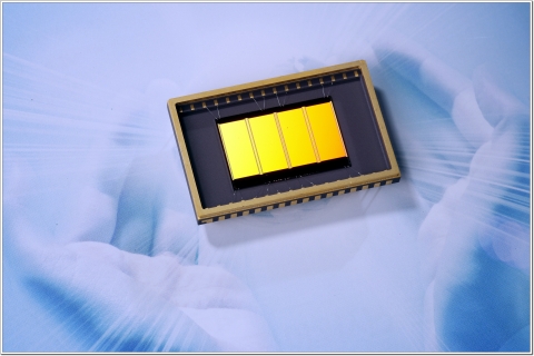
64G NAND Flash - ceramic pkg
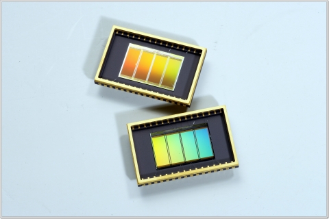
64G NAND Flash - ceramic pkg
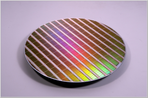
64G NAND Flash - wafer
The 30nm-class 64Gb NAND flash marks the eighth consecutive year that the density of memory has doubled and the seventh straight year that the nanometer scale has improved for NAND flash since the 100nm 1Gb NAND was developed in 2001.
The new flash device was successfully developed through the use of a new manufacturing process called self-aligned double patterning technology (SaDPT). In SaDPT, the 1st pattern transfer is a wider-spaced circuit design of the target process technology, while the 2nd pattern transfer fills in the spaced area with a more closely designed pattern. (Refer to image)
SaDPT represents a pivotal advancement beyond the charge trap flash (CTF) technology-based NAND flash that Samsung developed last year when it introduced a new material (silicon nitride) and a new structural configuration for flash memory. SaDPT resolves a critical bottleneck to forming sub-30nm circuitry by expanding the role that conventional lithography technology plays in the manufacturing process. Both Samsung’s CTF-based NAND flash technology and SaDPT are expected to provide improvements in cost efficiency for next-generation nanometer-scale designs.
Samsung’s SaDPT will employ existing photolithography equipment in 30nm production, which is expected to be commercialized beginning in 2009. By utilizing conventional photolithography equipment, Samsung can not only significantly speed up the process but also improve the cost efficiency of its manufacturing operations without additional facility investment. Samsung has applied for 30 patents in connection with the new 64Gb flash device.
Samsung also has developed a 32Gb single level cell (SLC) NAND flash memory based on the same technology applied to its 64Gb device. Samsung’s continued success in introducing higher density NAND flash will intensify demand for solid state drives in notebooks and other NAND-based storage devices for applications such as digital camcorders and enterprise servers.
Samsung expects to begin production of 30nm-class 64Gb flash devices in 2009. According to Gartner Dataquest, the accumulated sales for 64Gb NAND flash and higher density devices could reach up to $20 billion in just three years (2009~2011).
About Samsung Electronics
Samsung Electronics Co., Ltd. is a global leader in semiconductor, telecommunication, digital media and digital convergence technologies with 2006 parent company sales of US$63.4 billion and net income of US$8.5 billion. Employing approximately 138,000 people in 124 offices in 56 countries, the company consists of five main business units: Digital Media Business, LCD Business, Semiconductor Business, Telecommunication Network Business, and Digital Appliance Business. Recognized as one of the fastest growing global brands, Samsung Electronics is a leading producer of digital TVs, memory chips, mobile phones, and TFT-LCDs. For more information, please visit www.samsung.com
삼성전자 개요
삼성전자는 반도체, 통신, 디지털 미디어와 디지털 컨버전스 기술을 보유한 글로벌 리더다. 삼성전자는 디지털 어플라이언스 부문, 디지털 미디어 부문, LCD 부문, 반도체 부문, 통신 네트워크 부문 등 5개 부문으로 이뤄져 있다. 세계에서 가장 빠르게 성장하는 브랜드인 삼성전자는 스마트폰, 디지털 TV, 메모리 반도체, OLED, TFT-LCD 분야에서 세계 선두 주자다.
웹사이트: http://www.samsung.com/sec
연락처
Suyeon Chae
Tel : 82-2-727-7824
Email : 이메일 보내기

